

Masuk Bebas bergabung


1 / 5
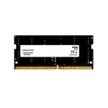
DDR4 Spesifikasi Modul Memori Udimm
| Model No. : | NS08GU4E8 |
|---|
Shenzhen, Guangdong, China
- Pabrikan
- Perusahaan perdagangan
- Pemasok Emas

- Sertifikasi Platform

- Ekspo online


Deskripsi Produk
8GB 2666MHz 288-pin DDR4 UDIMM
Sejarah Revisi
|
Revision No. |
History |
Draft Date |
Remark |
|
1.0 |
Initial Release |
Apr. 2022 |
|
Tabel Informasi Pemesanan
|
Model |
Density |
Speed |
Organization |
Component Composition |
|
NS08GU4E8 |
8GB |
2666MHz |
1Gx64bit |
DDR4 1Gx8 *8 |
Keterangan
Hengstar Unbuffered DDR4 SDRAM DIMMS (Tingkat Data Ganda DRAM DRAM DUAL MODUS DUAL IN-LINE) adalah modul memori operasi berkecepatan tinggi yang rendah yang menggunakan perangkat SDRAM DDR4. NS08GU4E8 adalah 1G x 64-bit satu peringkat 8GB DDR4-2666 CL19 1.2V SDRAM Produk DIMM Unbuffered, berdasarkan pada delapan komponen FBGA 8G x 8-bit. SPD diprogram ke Jedec Standard Latency DDR4-2666 Waktu 19-19-19 di 1.2V. Setiap 288-pin DIMM menggunakan jari kontak emas. SDRAM Unbuffered DIMM dimaksudkan untuk digunakan sebagai memori utama ketika diinstal dalam sistem seperti PC dan workstation.
Fitur
Pasokan kekuatan: VDD = 1.2V (1.14V hingga 1.26V)
VDDQ = 1.2V (1.14V hingga 1.26V)
VPP - 2.5V (2.375V hingga 2.75V)
VDDSPD = 2.25V hingga 3.6V
Terminasi on-die nominal dan dinamis (ODT) untuk sinyal data, strobe, dan topeng
Refresh self-power auto (LPASR)
Data Bus Inversion (DBI) untuk bus data
Di-Die VREFDQ Generasi dan Kalibrasi
Ton-board I2C Serial Presence-Detect (SPD) EEPROM
16 bank internal; 4 kelompok masing -masing 4 bank
Fixed Burst Chop (BC) dari 4 dan panjang burst (BL) dari 8 melalui set register mode (MRS)
Selectable BC4 atau BL8 on-the-fly (OTF)
Databus Tulis Cek Redundansi Siklik (CRC)
Refresh Refresh Terkendali (TCR)
Parity Perintah/alamat (CA)
Saha alamat drama didukung
8 Bit pra-Fetch
Topologi FLY-BY
Mommand/alamat latensi (CAL)
Command Bus Kontrol Terpisah dan Bus Alamat
PCB: Tinggi 1.23 ”(31.25mm)
Kontak tepi
Bohs yang sesuai dan bebas halogen
Parameter waktu utama
|
MT/s |
tCK |
CAS Latency |
tRCD |
tRP |
tRAS |
tRC |
CL-tRCD-tRP |
|
DDR4-2666 |
0.75 |
19 |
14.25 |
14.25 |
32 |
46.25 |
19-19-19 |
Tabel alamat
|
Configuration |
Number of |
Bank Group |
Bank |
Row Address |
Column |
Page size |
|
8GB(1Rx8) |
4 |
BG0-BG1 |
BA0-BA1 |
A0-A15 |
A0-A9 |
1 KB |
Diagram blok fungsional
Modul 8GB, 1GX64 (1Rank X8)

Peringkat maksimum absolut
Peringkat DC maksimum absolut
|
Symbol |
Parameter |
Rating |
Units |
NOTE |
|
VDD |
Voltage on VDD pin relative to VSS |
-0.3 ~ 1.5 |
V |
1,3 |
|
VDDQ |
Voltage on VDDQ pin relative to VSS |
-0.3 ~ 1.5 |
V |
1,3 |
|
VPP |
Voltage on VPP pin relative to VSS |
-0.3 ~ 3.0 |
V |
4 |
|
VIN, VOUT |
Voltage on any pin except VREFCA relative to VSS |
-0.3 ~ 1.5 |
V |
1,3,5 |
|
TSTG |
Storage Temperature |
-55 to +100 |
°C |
1,2 |
Rentang suhu operasi komponen drama
|
Symbol |
Parameter |
Rating |
Units |
Notes |
|
TOPER |
Normal Operating Temperature Range |
0 to 85 |
°C |
1,2 |
|
Extended Temperature Range |
85 to 95 |
°C |
1,3 |
Kondisi operasi AC & DC
Kondisi operasi DC yang direkomendasikan
|
Symbol |
Parameter |
Rating |
Unit |
NOTE |
||
|
Min. |
Typ. |
Max. |
||||
|
VDD |
Supply Voltage |
1.14 |
1.2 |
1.26 |
V |
1,2,3 |
|
VDDQ |
Supply Voltage for Output |
1.14 |
1.2 |
1.26 |
V |
|
|
VPP |
Supply Voltage for DRAM Activating |
2.375 |
2.5 |
2.75 |
V |
3 |
Dimensi modul
Tampak depan

Tampak belakang


Shenzhen, Guangdong, China
- Pabrikan
- Perusahaan perdagangan
- Pemasok Emas
- Sertifikasi Platform
- Ekspo online
Kirim pertanyaan Anda ke pemasok ini